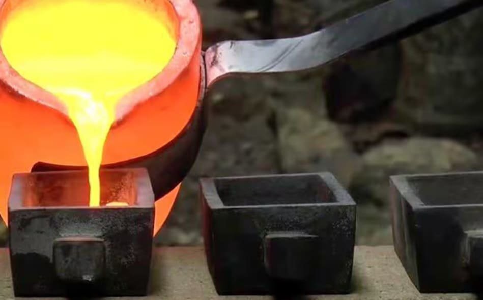
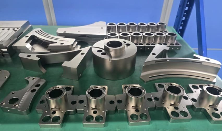
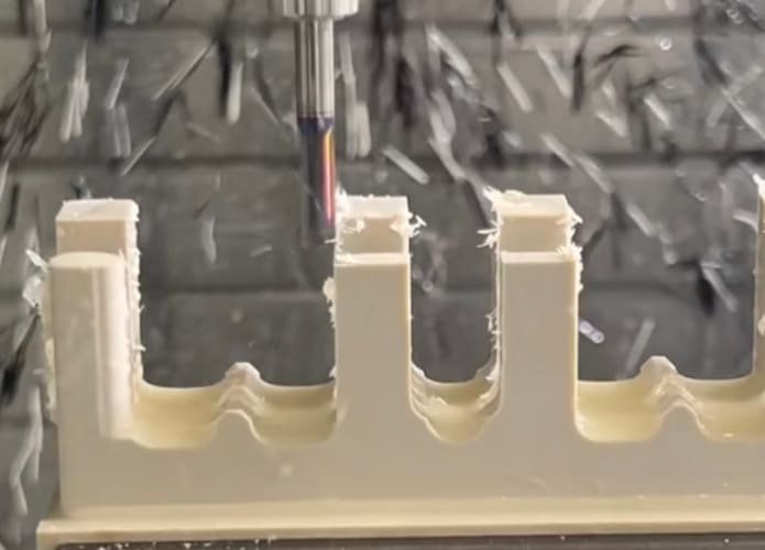
Manufacturing semiconductor parts is a real challenge. Every part must meet strict standards of precision, tolerances and surface quality. CNC machining fulfills these needs with accuracy & dependability. In this blog post we will explain the role of CNC machining in the semiconductor sector, highlight the key techniques used and share best practices to get high quality results.
The Critical Role of CNC Machining in Semiconductor Manufacturing
Semiconductor fabrication represents one of the most demanding manufacturing environments in the world. The production of microchips requires components machined to micron-level tolerances, with surface finishes measured in nanometers. Traditional manufacturing methods simply cannot meet these exacting standards consistently.
Advanced CNC machining systems deliver the precision, repeatability, and cleanliness that semiconductor production demands. From wafer handling components to vacuum chamber parts, CNC machining creates the infrastructure that makes modern electronics possible.
Key Applications of CNC Machining in Semiconductor Production
CNC machining supports virtually every stage of semiconductor manufacturing, from initial wafer processing to final testing.
Vacuum Chambers and Housings
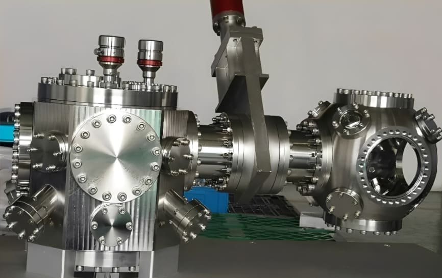
Semiconductor fabrication occurs in ultra-clean vacuum environments. CNC machined vacuum chambers, typically made from aluminum or stainless steel, must maintain perfect seals while accommodating complex internal geometries for gas distribution, electrical connections, and optical systems.
Wafer Handling Components
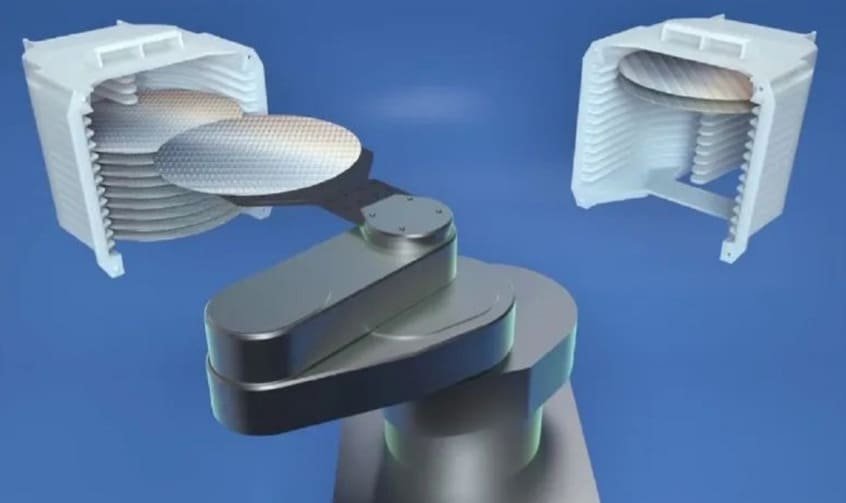
Silicon wafers are extremely fragile and sensitive to contamination. CNC machined handling systems, including robotic end effectors, transfer arms, and alignment fixtures, must be lightweight yet rigid, with smooth surfaces that won’t generate particles or damage wafers.
Chemical Vapor Deposition (CVD) Components
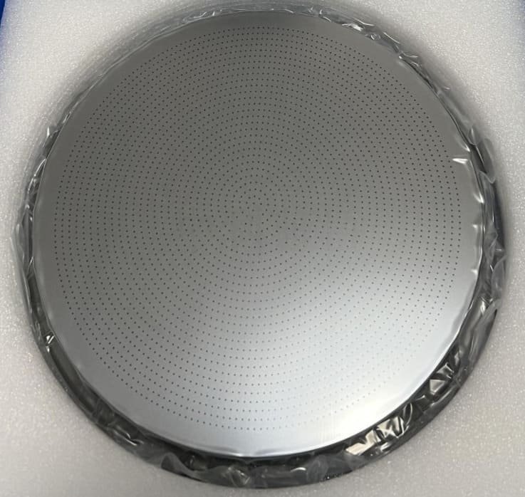
CVD shower heads distribute process gases uniformly across wafer surfaces. These components feature thousands of precisely sized and spaced micro-holes, often in complex patterns that require high-speed spindles and specialized micro-tooling to manufacture.
Test Sockets and Fixtures
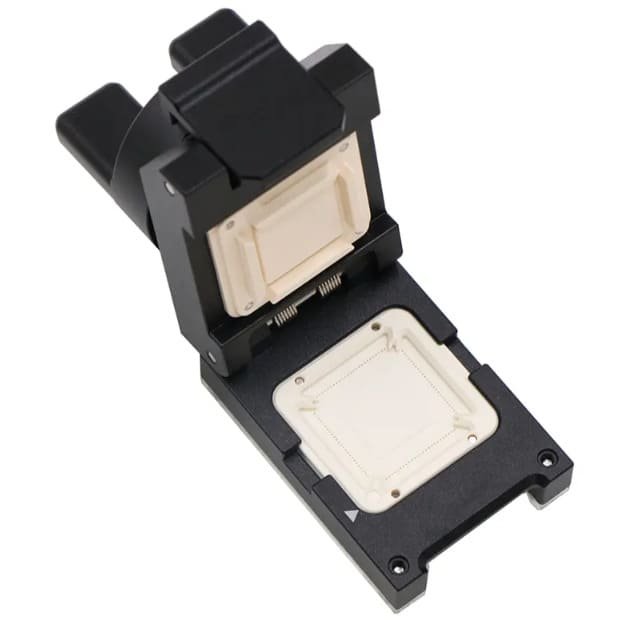
Before packaging, semiconductor chips undergo rigorous testing. CNC machined test sockets, typically made from engineering plastics like PEEK or PEI, require ultra-precise micro-hole arrays to house contact pins that interface with chips.
Polishing Pad Molds
Chemical-mechanical planarization requires extremely smooth, flat surfaces. CNC machined aluminum molds with mirror-like finishes ensure consistent polishing pad production for this critical process.
Heater Plates
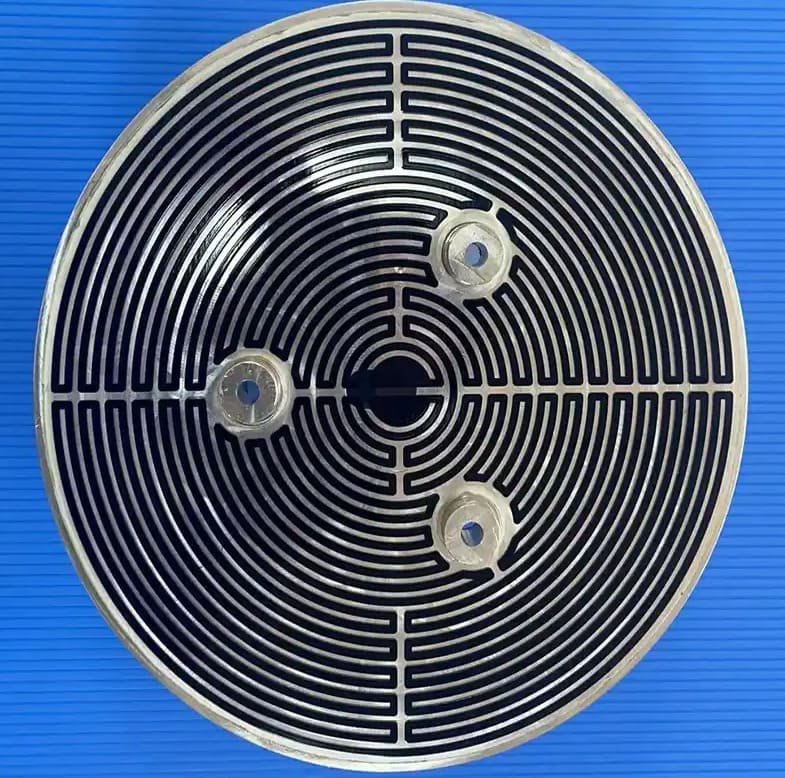
Temperature control is essential in semiconductor processing. CNC machined heater plates with integrated cooling channels maintain precise thermal conditions during manufacturing.
Material Considerations for Semiconductor-Grade Components
| Material | Common Applications | Advantages | Machining Considerations |
| Aluminum (6061-T6) | Vacuum chambers, fixtures, wafer handling. | Lightweight, excellent thermal conductivity, low outgassing. | High-speed machining with ethanol-based coolant for residue-free surfaces. |
| Stainless Steel (316L) | Vacuum components, gas delivery systems. | Excellent corrosion resistance, high strength, low magnetic permeability. | Requires rigid machine tools and optimized cutting parameters. |
| PEEK (Polyether Ether Ketone) | Test sockets, insulators, fixtures. | Excellent chemical resistance, low outgassing, high temperature stability. | Specialized tooling and parameters to prevent heat damage. |
| Ceramics (Alumina, Silicon Carbide) | Wafer supports, heater components. | Extreme hardness, temperature resistance, dimensional stability. | Requires specialized diamond tooling and rigid machine platforms. |
The semiconductor industry increasingly requires exotic materials like molybdenum, tungsten, and specialized ceramics for extreme environment applications. CNC machining these materials demands specialized tooling, rigid machine platforms, and extensive process optimization.
Precision and Tolerance Requirements for Semiconductor Equipment
Semiconductor manufacturing operates at the microscopic level, requiring machining tolerances that push the boundaries of conventional CNC capabilities. Understanding these requirements is essential for successful component production.
Dimensional Tolerances
Many semiconductor components require tolerances of ±0.005mm (5 microns) or tighter. Achieving these specifications demands thermally stable machine platforms, high-precision spindles with minimal runout, and advanced in-process measurement systems.
Geometric Tolerances
Beyond simple dimensional accuracy, semiconductor components often require exceptional flatness, parallelism, and perpendicularity. Vacuum sealing surfaces, for example, may specify flatness tolerances of 0.01mm across large areas.
Surface Finish Requirements
Surface roughness in semiconductor applications is typically specified in nanometers rather than microinches. Components that contact wafers or influence gas flow patterns may require Ra values of 0.2μm or better, necessitating specialized tooling and machining strategies.
Surface Finish and Cleanliness Standards for Contamination Control
Contamination control represents one of the most critical aspects of semiconductor manufacturing. Even microscopic particles can render chips useless, making cleanliness essential throughout the production process.
Machining Considerations for Cleanliness
Conventional machining processes using oil-based coolants can leave residues that compromise semiconductor processes. Advanced CNC systems for this industry often utilize:
- Ethanol-based cooling systems that evaporate without residue.
- Enclosed machining environments with HEPA filtration.
- Specialized tool holders and collets that minimize particle generation.
- Vacuum chip extraction systems that prevent recontamination.
Post-Machining Cleaning Protocols
Even with clean machining processes, semiconductor components typically undergo rigorous cleaning procedures before use. These may include ultrasonic cleaning, vapor degreasing, plasma cleaning, and cleanroom packaging to maintain surface integrity.
Key CNC Machining Methods for Semiconductor Parts
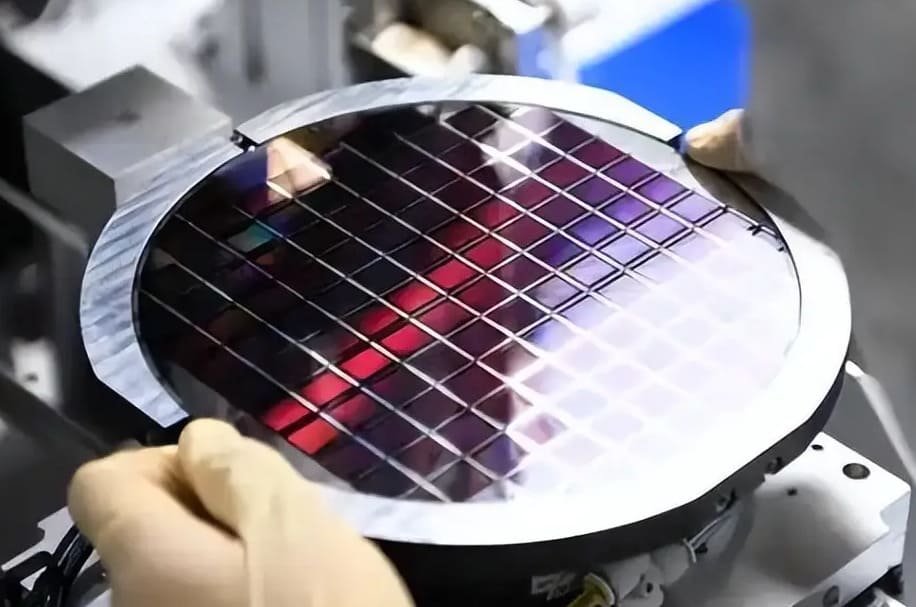
To produce semiconductor components with the needed precision and quality, different advanced CNC machining techniques are employed.
1. Precision Milling & Micro-Machining
Precision milling is used to shape complicated semiconductor parts by removing material with small, high speed cutting tools. This method provides extremely high accuracy.
Micro-milling is a more specialized approach that creates ultra-small features—often smaller than 1 millimeter. This technique is important for manufacturing sensor housings and microelectronic parts.
2. Precision Turning & Micro-Turning
Manufacturers use precision turning to produce cylindrical parts for semiconductors. In this process, the workpiece is rotated while a fixed cutting tool shapes it. Micro-turning applies the same method to parts with extremely small diameters such as shafts & pins. Both techniques help achieve tight tolerances and superior surface finishes.
3. Drilling, Micro-Hole Fabrication & Features for Semiconductor Equipment
Accurate features and holes are critical for the proper operation of semiconductor equipment.
- Drilling: This method creates channels that allow the flow of fluid or gas and forms electrical pathways in parts such as showerheads.
- Micro-Hole Fabrication: Professionals use advanced methods like ultrasonic or laser drilling to produce extremely small holes. These holes, often less than 0.5mm in diameter, are vital for parts such as gas distributor plates.
4. Material-Specific Machining (Composites, Ceramics, Exotic Alloys)
Technical composites, ceramics as well as exotic alloys are commonly used in semiconductor components. These advanced materials are difficult to machine and need special techniques to prevent damage. For hard ceramics such as Alumina (Al2O3) and Silicon Carbide (SiC), diamond tools are often used.
5. Cleanroom & Contamination-Controlled Machining
Machining semiconductor parts must be done in a cleanroom environment with strict contamination control. Powerful ULPA and HEPA filters remove airborne particles from the surroundings. This step prevents defects in sensitive microchips. Workers follow strict protocols, such as using electrostatic discharge (ESD) controls and wearing protective suits, to maintain the purity of components.
Best Practices & Process Considerations
CNC machining in the semiconductor sector demands extremely high precision. Following the best practices is fundamental to assure reliable performance of small parts.
Design for Extreme Precision
When working with semiconductors, success depends on precise design. For parts like wafer chucks you should set micron-level tolerances. Use Design for Manufacturability (DFM) to address the challenges of micro-machining. Involve machinists early in the design process as it will assure practicality and help avoid costly errors.
Select & Maintain High-Precision Equipment
The quality of your machines and tools determines the quality of the final part. Choose CNC machines with high rigidity plus good quality micro-tools that are designed for detailed features. Also, regularly calibrate equipment to avoid deviations that can damage valuable components.
At CNCPOR, our 5-axis, high-rigidity CNC machines are routinely calibrated. This assures premium accuracy for small-features.
Optimize Machining Parameters for Delicate Work
Careful selection of machining parameters is crucial to protect fragile materials. Use CAM software to create smooth toolpaths—this prevents micro‐fractures. Adjust feeds and speeds for brittle materials or small features. These steps help achieve flawless surface finishes appropriate for demanding applications.
Implement Rigorous Quality & Process Control
Strict quality control is essential for reliable parts. Therefore inspect micron‐level features using advanced tools such as Coordinate Measuring Machines (CMMs). Use Statistical Process Control (SPC) to monitor production and detect issues early. This approach prevents defects and maintains complete traceability.
Enforce Strict Cleanliness & Contamination Control
In semiconductor manufacturing, contamination is unacceptable— even a single particle can destroy a silicon wafer. Therefore use multi-stage cleaning to remove unwanted oils and microscopic debris. Handle and package finished parts in a cleanroom environment to keep them free from recontamination.
Adopt Flexible High-Mix/ Low-Volume (HMLV) Strategies
In the semiconductor industry, small batches of custom parts are common. Using HMLV strategies is the most effective way to meet this demand. Flexible CNC setups and automation allow for fast job changeovers. This approach keeps costs low for small, specialized batches used in research, development or other unique equipment.
CNCPOR‘s modular fixturing systems and lean setups minimize changeover time. This makes us an ideal machining partner for urgent development work or lab-scale runs.
Challenges & Solutions in CNC Machining for Semiconductor Applications
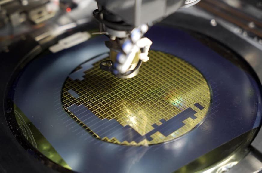
1. Maintaining Ultra-Tight Tolerances & Surface Finishes
Maintaining tolerances within microns is always challenging. Even minor temperature shifts can affect precision.
To overcome this issue, use ultra-precise machines and maintain a climate-controlled workspace. Advanced tool holders and vibration-damping systems add further stability. These measures assure that every part meets stringent tolerances such as ±0.0025 mm.
2. Machining Difficult Materials
Semiconductor components often require hard or brittle materials such as ceramics and composites. These materials tend to crack or chip easily and cause rapid tool wear.
Specialized cutting tools, such as polycrystalline diamond (PCD) coated tools, offer an effective solution. Ultrasonic-assisted machining is also beneficial because it reduces stress on the workpiece.
3. Cycle Times, Throughput Vs Quality Trade-Offs
It’s necessary to balance production speed and quality. This is because rushing can lead to defects while slower operations can harm throughput.
High-speed machining and optimized tool paths can be adopted to reduce cycle times while maintaining accuracy. Moreover, automating repetitive steps lets operators focus more on quality checks.
4. Cleanroom Compatibility & Contamination Risk
A spotless manufacturing environment is mandatory. Oil or dust generated during machining can contaminate sensitive parts and lead to device failures. To prevent this, use equipment and coolants designed for cleanrooms and avoid any residue. Strict inspection and cleaning routines are vital to keeping contamination under control.
CNCPOR’s team uses cleanroom-compatible coolants and residue-free finishing methods to assure all interfaces connected to optics or vacuum assemblies remain secure.
5. Cost Control & Predictable Quality for Small Batches
Small and custom batches are often more expensive because setup takes longer.
USe Modular fixtures and standardized routines to speed up changeovers. Running machining simulations before production also reduces material waste and errors. These measures make small‐batch jobs more cost-effective.
To Sum Up
The semiconductor industry depends on CNC machining for its advancement. This technology provides the high precision, complicated geometries and consistent quality required for advanced electronics. If you need custom semiconductor parts produced quickly and to the highest purity standards, CNCPOR is the top choice. You can contact us anytime.
Related Questions
What unique fixturing or workholding methods are needed for CNC machining semiconductor parts?
Specialized fixtures are necessary for these parts. Vacuum chucks and other non‐contact options help prevent contamination and protect delicate materials from warping.
Is it possible for CNC machining to produce micro-scale features like dense hole arrays in semiconductor equipment?
Micro-CNC machining is specifically designed for this purpose. It can achieve extremely small and complicated features with tight tolerances needed for semiconductor parts.
Why is it vital to monitor tool wear and run-out in semiconductor CNC machining?
Controlling tool wear & run-out is critical. These factors affect surface finish quality and dimensional accuracy, both of which are necessary for the performance of semiconductor parts.
Which failure types must CNC shops prevent when machining semiconductor parts?
Shops must avoid issues such as incorrect dimensions, small defects and rough surface finishes that can arise under thermal or electrical stress.
How does CNC machining work alongside other manufacturing processes like laser, EDM or additive methods for semiconductor parts?
CNC machining typically shapes the main parts and housings used in the semiconductor field. Processes such as EDM or laser machining are then applied to add ultra‐fine features that standard CNC tools cannot produce.

